
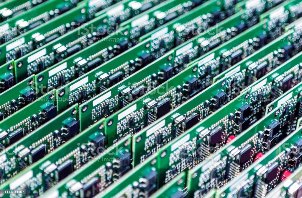
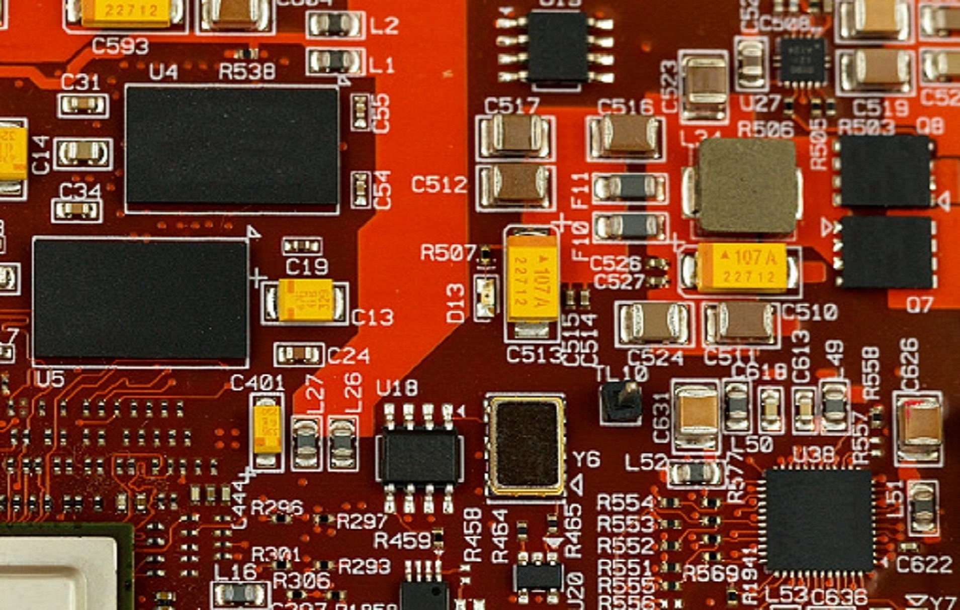
Electronics' PCB signal integrity is a crucial component. This is influenced by a variety of parameters, such as crosstalk, reflection, attenuation, and delay. Understanding these elements and how they might be applied to improve performance is crucial for properly protecting a design.
Crosstalk
Two PCB nets that are electromagnetically connected may experience a phenomena called crosstalk. Electric and magnetic forces at the fringes are what are causing this interference.
One signal producing a burst of current at the same time as another signal that shares the same properties is a classic example of crosstalk. In response, the victim signal develops an unwanted signal.
Increasing the separation between the two signals is one method for reducing crosstalk. Increasing the separation between the two signals will not only increase the quality of the victim signal but also lessen the crosstalk caused by the victim signal.
Eliminating parallel traces between layers is another method for reducing crosstalk. There may be a very slight vertical coupling between the layers as a result of these overlapping signals.
A PCB can avoid creating crosstalk by adhering to a few straightforward design guidelines. First, the distance between signals needs to be wide enough to prevent the previously described modest vertical coupling. Second, to avoid the aforementioned connection, solid planes should be used instead of voids.
Reflection
Engineers must pay close attention to a circuit's signal integrity throughout the PCB design process. The capacity of an electrical signal to transmit without distortion is referred to here.
There are a few actions to think about taking in order to achieve this. The first step is to confirm that the line's impedance matches that of the signal trace.
Terminations can be used to accomplish this. Both the source and the destination of the connection can accommodate these devices.
The board's material's dielectric constant, the width of the signal trace, and the separation between the trace and the reference plane are additional factors to take into account. By selecting the right materials, one may prevent electromagnetic interference (EMI) and other issues from affecting the PCB.
Attenuation
An key PCBsignal integrity issue is signal attenuation. The signal's attenuation is influenced by a number of variables. These consist of the trace resistance, the conductor material, and the dielectric losses. The amount of amplitude reduction at the receiver increases with increasing attenuation values.
Choosing the right materials will make it simple to avoid the signal attenuation issue. For instance, surface spikes caused by rough copper traces can have an impact on the signal. High-speed, low-loss materials can also be useful. A repeater device can be used to avoid attenuation as well.
Lengthening the signal and expanding the conductor area are two other methods for reducing attenuation. Engineers can locate the issue's root cause by measuring attenuation with a vector network analyzer. The PCB will operate flawlessly at high frequency if the attenuation issue can be avoided.
Delay
The signal integrity must be taken into consideration while designing a PCB. A well-designed PCB will prevent signal deterioration brought on by ground bounce and attenuation. The performance of the PCB will be impacted if there are any signal issues.
How a PCB handles signals during the design and manufacturing processes determines the signal integrity of the PCB. The board material, transmission line impacts, and circuit design are only a few of the variables that affect signal integrity.
The length and impedance of the traces must both be taken into account when designing a PCB. Especially for high-speed PCB, this is crucial. The shortest and straightest traces will have the least delay.
The rise/fall time of the signal must be at least equivalent to the one-side propagation delay for high-speed PCB. The signal will be corrupted if the rise/fall time is shorter than the propagation delay.
System integration
To ensure signal integrity while designing PCBs for high frequency applications, is crucial. This is because the signal travels through the substance at the speed of light. Although it cannot be prevented from reaching the receiver, several factors can reduce the quality of the signal.
Engineers should be familiar with the fundamental guidelines and methods utilised in the design in order to prevent signal integrity problems in PCBs. These methods aid designers in finding circuit-level issues.
Engineers can lessen the effects of these signal interference problems during the initial design stages. Additionally, they can stop costly design iterations.
Signal integrity testing is a typical activity throughout the board designing stage. Signal deviations can be found by engineers using a spectrum analyzer. Engineers can save money and save needless design iterations by spotting and fixing these issues early in the project cycle.

No comments yet